Leading the photolithography field
Photolithography makes it possible to build polymer microstructures on a thin wafer—similar in some regards to additive manufacturing. The most obvious photolithography application is silicon chips. But the process is used in many different applications for scientific research.
Raymax represents French lithography manufacturer KLÓE for academic research in Australia and New Zealand. They offer a range of robust mask aligners and direct laser writing systems. Discover the advantages of each and how photolithography is making scientific and production advancements possible. Learn more about our custom solutions here.
Read more about Kloe here.
What photolithography machine is right for you?
Whether you’re looking for a mask aligner, direct laser writing equipment, or high-resolution 3D microfabrication, Raymax (together with KLÓE) can support you. KLÓE’s mask aligner systems allow you to quickly and accurately reproduce set patterns using a mask. The UV light beams down and replicates that set pattern in the resist. Each copy can be achieved within a billionth of a second. This is ideal for applications where you need speed and accuracy but aren’t looking to change the pattern or aspect ratio regularly.
Build with high-aspect ratios
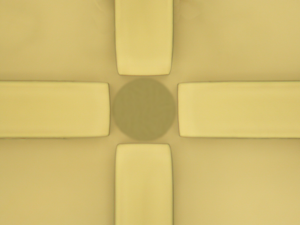
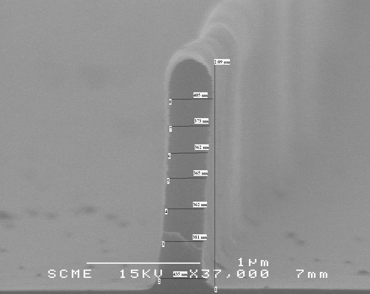
For those lithography applications where you need to build with a high-aspect ratio of 30:1, for example, KLÓE’s range of direct laser writing equipment is ideal. Some examples include nanoelectronics, microfluidics, photonics, surface functionalisation, 3D biotechnology, micromechanics, and greyscale levels. This software-driven technology runs the laser (1-, 5-, or 10-micron in diameter) over the resist in a true vector writing mode. You don’t have to change the mask every time you need a new pattern or aspect ratio. You simply change it in the software. This freedom is crucial in microfluidics. The resulting structures are completed with greater accuracy, depths of focus, and structural integrity.
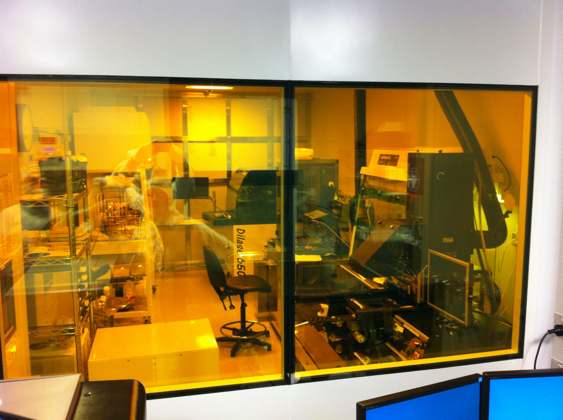
“The ANFF-SA node routine uses their Dilase 650 system to support the cutting-edge research conducted within the facility.
Lab on a chip
Lab on a Chip is a good example of the small features and intricate capabilities made possible with lithography. Finding better ways to create complex patterns and pathways in a chip less than a millimetre wide is crucial to the research and development within microfluidics. By processing small amounts of fluid in microchannels, what once was only possible in a lab is now possible on a chip. Hence the name: Lab on a Chip. KLÓE photolithography machines create these chips with precision additive technology.
Greater precision
KLÓE responded to the call from researchers, like you, for thicker photoresists with their Dilase range. Now it’s possible to write with precision in thick layers. You can also achieve perfect quality on the written sidewalls. The dynamically controlled stages make sure the structures created by the photolithography machine are accurate. The stages feedback any changes (for example, change in temperature) to the controller to adjust accordingly. So you get reliable motion and reliable results.
Why Raymax?
We make laser light work for you. We’ve spent over 30 years demonstrating what’s possible with lasers. In doing so, we’ve helped modernise Australian and New Zealand industries. You’ll be working with a team of physicists and factory-trained engineers—leaders in the supply of laser solutions and photonics equipment. We’re experts in material interaction research. Wherever possible, you’ll be introduced to new technology that can improve operation in ways you might not have imagined possible.
Speak to an expert
Enter your details and we’ll get in touch to discuss your needs.Book a Consultation
Contact Us
(02) 9979 7646
Visit Us
37/5 Ponderosa Parade Warriewood NSW 2102